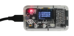
SC LINK PRO is designed for offline/online programming & simulation and TouchKey debugging of SC92F/93F/95F series MCU
Products
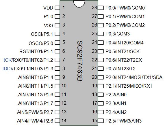
SC92F7463B
Operating Voltage: 2.4V ~ 5.5V
Operating Temperature: -40 ~ 85℃
Package:
SC92F7463B (SOP28/TSSOP28)
Core: 1T 8051
Flash ROM: 16K bytes Flash ROM (MOVC) prohibited addressing 0000H ~ 00FFH) can be rewritten for 10, 000 times
IAP: Code option into 0K, 0.5K, 1K or 16K
EEPROM: 128 bytes EEPROM can be rewritten for 100, 000 times. The data written-in has more than 10-year preservation life.
SRAM: Internal 256 bytes + external 768 bytes
System Clock (fSYS):
l Built-in high-frequency 16MHz oscillator (fHRC):
n As the system clock source, fSYS can be set to 16/8/4/1.33MHz by programmer selection.
n Frequency Error: Suitable for 3.0V ~ 5.5V and -20 ~ 85℃ application environment, no more than ±1% of frequency error
l Built-in high-frequency Crystal Oscillator Circuit
n Available to externally connect 2-16 MHz Oscillator
n As the source of system clock, fSYS can be set to /2, /4 or /12 of the frequency of oscillator via code option.
l Operating voltage at different system frequency:
Built-in Low-Frequency 128kHz Oscillator (LRC):
l Clock source of Base Timer (BTM), which can wake up the SC92F746XB from stop mode
l Clock source of Watchdog (WDT)
l Frequency Error: 4.0V ~ 5.5V and -20 ~ 85℃ application environment, no more than ±4% of frequency error
Low-voltage Reset (LVR):
l 4-level LVR voltage options: 4.3V, 3.7V, 2.9V, 2.3V
l The default is the Code Option value selected by the user
Flash Programming and Emulation:
l 2-wire JTAG programming and emulation interface
Interruption (INT):
l 11 interrupt sources: Timer0, Timer1, Timer2, INT0 ~ 2, ADC, PWM, UART, SSI and Base Timer.
l 3 external interrupt vectors shared by 13 interrupt ports, all of which can be defined in rising-edge, falling-edge or dual-edge trigger mode.
l Two-level interrupt priority capability
Digital Peripheral:
l Up to 26 bidirectional independently controllable I/O interfaces, able to configure pull-high resistor independently
l P0/P2 ports with 4-level drive capability
l All I/Os equipped with sink current drive capability (70 mA)
l 11-bit WDT with optional clock division ratio
l 3 standard 80C51 Timer/Counters: Timer0, Timer1 and Timer2
l Timer2 can be set to capture mode
l Six 10-bit PWM output channels with variable period and individual duty cycle, which can simultaneously output three sets of complementary PWM waveforms with dead zone
l 5 I/Os as output of the 1/2-bias LCD COM
l 1 independent UART communication interface (Switchable I/O port)
l 1 three-in-one serial communication interface (SSI) (Switchable I/O port)
l 16*16-bit hardware multiplier and divider unit (MDU)
Analog Peripheral:
l 11-channel 12-bit ±2LSB ADC
n Built-in 2.4V reference voltage
n 2 options for ADC reference voltage: VDD and internal 2.4V
n Internal one-channel ADC, where VDD can be measured directly
n ADC conversion completion interrupt
Power Saving Mode:
l IDLE Mode: can be woken up by any interrupt.
l STOP Mode: can be woken up by INT0 ~ 2 and Base Timer