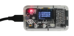
SC LINK PRO is designed for offline/online programming & simulation and TouchKey debugging of SC92F/93F/95F series MCU
Products
SC95F8615
建议使用SC95F8615B产品
Operating Conditions
l 2.0V~5.5V Vcc Voltage Range
l -40℃ ~ +105℃ Temperature Range
ESD&EFT
l ESD 6KV
l EFT 4KV
Package
l 32 PIN: LQFP32 (7X7) / QFN32 (5X5)
CPU
l Super-high-speed 1T 8051 core
l The instruction set compatible with 8051
l The execution speed is about twice that of other 1T 8051
l Double data pointers (DPTRs)
Storage
l 64K bytes Flash ROM
n Divided into 128 sectors
n 512 bytes per sector
n Can be rewritten 100,000 times
n The data written-in has more than 100-year preservation life in the ambient temperature of 25℃
l IAP (In Application Programming): The area allowed IAP operation in Flash can be set to 1/2/4/64K by Customer Option.
l Encryption: APROM and LDROM can be encrypted to ensure that the program code cannot be read
l BootLoader: Built-in 1K bytes LDROM
l Unique ID: 96 bit unique ID memory
l SRAM: Internal 256 bytes + external 4K bytes + PWM&LCD RAM 80 bytes
Flash Programming and Emulation
l 2-wire JTAG programming and emulation interface
l Mass production burning: 64 Kbytes of Flash ROM burning and verification total time can be as low as 2s
Clock Source
l Built-in high frequency 32MHz oscillator (HRC)
n The system clock frequency (fsys) of the IC can be selected and set by the programmer as: 32/16/8/4MHz
n Frequency Error:
u Within ±1% @ -10 ~ 85℃
u Within ±2% @ -40 ~ 105℃
n The system clock can be automatically calibrated by 32.768kHz external crystal oscillator, after calibration HRC accuracy can be infinitely close to the accuracy of external 32.768kHz crystal oscillator.
l Built-in low-frequency crystal oscillator circuit: 32.768k oscillator can be connected externally as a Base Timer clock source.
l Built-in low-frequency 32kHz oscillator (LRC): used as the clock source for Base Timer and WDT.
Low-voltage Reset (LVR)
l 4 options of reset voltage: 4.3/3.7/ 2.9/1.9V, the default value can be selected by the Customer Option
Interrupts (INT)
l Up to 17 interrupt sources including Timer0~Timer4, INT0~2, ADC, PWM, UART, USCI0~2, Base Timer, TK, CMP
l External interrupt INT0~2 contains 3 interrupt vectors, 16 intermediate fractures. All can set up rising edge, falling edge, double edge interrupt.
l Two-level interrupt priority capability
Digital Peripheral
l GPIO
n Up to 30 bidirectional independently controllable I/O ports, independent setting of pull-up resistors
n All I/Os have large sink current drive capability (50mA)
l Built-in WDT, optional clock frequency division ratio
l 5 Timers: Timer0~4
l 8-channel 12-bit PWM
n Can be set to independent mode or complementary mode: 8 channels of PWM in the independent mode, the duty cycle can be set separately
n In complementary mode, four sets of complementary PWM waveforms with dead zones can be output simultaneously
n The output waveform can be reversed and can be set to center-aligned or edge-aligned
n Fault detection mechanism
l One independent UART communication port UART0
l Three UART/SPI/TWI communication interfaces (USCI)
l Integrated with 16 * 16-bit hardware Multiplier-Divide Unit (MDU)
l Built-in CRC check module
l LCD/LED driver
n Choose one of two LCD/LED drive functions, share registers and I/O ports
n LED driver: 8 X 28, 6 X 26, 5 X 27, or 4X 28 segments, LED segment port (P0~P3) source drive capability is selectable in four levels
n LCD driver: 8 X 28, 6 X 26, 5 X 27, or 4X 28 segments
Analog Peripheral
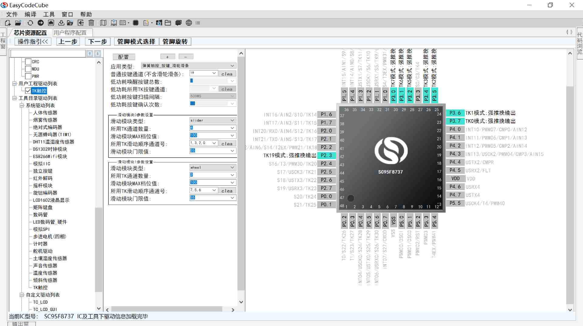
l 19-channel dual-mode TouchKey (TK) circuit.
n High-sensitivity mode applicable to TouchKey sensor, proximity induction and other TouchKey applications featuring high requirements on sensitivity
n High reliability mode features very strong anti-interference which is able to pass 10V dynamic CS test
n Support self-capacitance programme and reciprocal- capacitance mode.
n Support low power consumption mode.
n Complete development support: High-flexible touch software library, intelligent software of debugging.
l 9-channel 12-bit high-speed ADC
n 1MHz sampling clock
n The ADC reference voltages is optional:
u Internal 2.048V
u Internal 1.024V
u VDD
n One internal channel can measure the voltage of the power supply
l 1 Analog Comparator
n 4-channel input and 1-channel reference voltage input
n 16-level optional comparison voltage
Power Saving Mode
l Normal Mode: current consumption is as low as 5.2mA (VDD=5V, fsys=32MHz)
l IDLE Mode: current consumption is as low as 2.5mA (VDD=5V), can be woken up by any interrupt
l STOP Mode: can be woken up by INT0~2, Base Timer and TK.